
This is non-commercial site, its content is based on Atari 8-bit home computer contents and references.
If you feel your rights are violated by showing/using any part of contents of your product represented on this page,
please contact me immediatelly so I can remove it!

Atari 8-bit Hardware
|
|
|
|
-
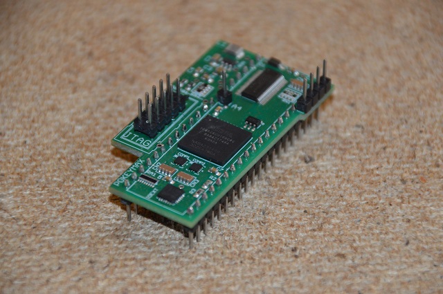
Entry name:PokeyMAX
-
Category:Music/Speech/Digitizer
-
Manufacturer:ABBUC e.V., ABBUC Hardware Contest 2018
-
Year:2018
Short description
Introduction The PokeyMAX is a complete replacement for the Pokey chip. It is derived from the work on the EclaireXL project, a complete FPGA based Atari 800XL clone. The intention is to build replacements for all of the Atari custom chips using this technology and Pokey has been built first. It can be used either to replace a broken/missing pokey, as a stereo upgrade, or just for fun! Features ï‚· If pokey is socketed, zero wire installation (mono) ï‚· Dual pokey mode ï‚· Pins for 3 audio outputs (left channel/right channel/mixed) ï‚· Small footprint, only a few mm larger than original IC ï‚· Supports all features: 8x paddle inputs, IRQ, serial I/O, audio output, two tone mode, high pass filter and keyboard scan ï‚· High level of compatibility Digital logic The PokeyMAX is built around the Altera MAX10 FPGA. This was chosen due to its integrated flash memory, power conversion, small size and low cost. The contained logic itself is described in VHDL and Verilog and then synthesized using the Quartus II software. Level conversion Most modern FPGAs no longer support 5V logic. While it is possible to find a few they are a vanishing breed. The MAX10 only supports up to 3.3V logic, so an IDT quickswitch level converter IC is used to connect to the high speed lines (A/D/IRQ/serial io etc) safely. Chip select Unfortunately I needed more level conversion lines than provided. TI came to the rescue with some 5V tolerant multi-function logic chips with which I was able to combined CS/!CS into one. Power The MAX10 requires a single 3.3V power supply, it then internally generates the rest of its supplies. This is very convenient, since often FPGAs require 3 or more different voltage levels. There is a switch mode regulator (LM3670) to convert from 5V to 3.3v in an efficient fashion. Paddles These are handled by charging a capacitor that we then check the level of using an LMV339. This is similar to the well-known LM339 comparator, except much smaller! The comparator is used since the level can be set very precisely rather than relying on when the FPGA detects a logic high. The level itself is set to 2.2v using the voltage divider on the right. It is also convenient since its open drain output means there are no level conversion issues. For the drain transistors, a 5V tolerant IO extender chip is used. The FPGA communicates with this over an I2C bus. Keyboard scan An IO extender chip drives the 6 keyboard lines and then reads the response. This is convenient since it only requires an I2C bus to the FPGA and the IC is much smaller than the level converters. JTAG The Ä‚Ë€˜coreÄ‚ËĂ˘â€šÂ¬Ă˘â€žË may be upgraded or debugged using an Altera USB blaster connected here. Several of the JTAG pins are Ä‚Ë€˜dual useÄ‚ËĂ˘â€šÂ¬Ă˘â€žË and can be used as general IO. So we could for instance in future plug in i2c devices here or use for A5 (with external level converter) to allow quad pokey or sid etc. Audio filter The audio output uses a delta sigma dac. An RC circuit is used as a simple audio filter to smooth the output from this. There are four audio outputs, which are currently fed to pin 37 and 3 header pins (left/right and mixed). Note that the next stage much not draw a lot of current from the rc filter or it will cause distortion. A4 Pokey has 4 address pins (A0-A3). To make space for a 2nd pokey another address line is needed. For stereo connect to A4. Source: http://www.abbuc.de http://www.abbuc.de/community/forum/viewtopic.php?f=15&t=9560#p79419
References
Copyright holder